The Machine That Saved Moore’s Law: How ASML Revolutionized Chip Manufacturing with Extreme Ultraviolet Lithography
For over half a century, Moore’s Law—the observation that the number of transistors on a microchip doubles approximately every two years—has driven the exponential growth of computing power. This relentless miniaturization has transformed technology and society. But around 2015, the progress of shrinking transistors nearly hit an insurmountable barrier. The solution? A staggering feat of engineering: an extreme ultraviolet (EUV) lithography machine, developed by a single company, ASML. This machine not only saved Moore’s Law but also became arguably the most complex commercial product ever built.
The Challenge of Making Smaller Microchips
Microchips start with purified silicon, which is formed into large single-crystal ingots and sliced into wafers. Each wafer is then layered with intricate patterns using photolithography—a process where light passes through a patterned mask to etch designs onto the silicon. This patterning defines the tiny transistors and metal wires that make up a chip.
However, as chip features shrank, traditional photolithography using deep ultraviolet light (~193 nm wavelength) reached a physical limit. The wavelength of light used determines how small features can be printed; when features approach the wavelength size, diffraction and interference effects distort the patterns. To print smaller features, either the lens system’s numerical aperture must increase (impractical beyond certain limits) or the wavelength must be shortened.
Enter Extreme Ultraviolet Lithography (EUV)
In the 1980s, scientist Hiroo Kinoshita proposed using extreme ultraviolet light with a wavelength around 13.4 nm—about 15 times shorter than deep UV light—to print much smaller chip features. This idea faced enormous obstacles:
- Light Absorption: EUV light is absorbed by almost all materials and even air, requiring the entire process to occur in a vacuum.
- No Lenses: Conventional lenses absorb EUV, so the system must use specially designed multilayer mirrors to reflect and focus the light.
- Mirror Smoothness: The mirrors must be atomically smooth to avoid scattering EUV light, with surface roughness controlled down to just a few atoms.
Despite skepticism and initial failures, progress continued, fueled by research from Lawrence Livermore National Laboratory (LLNL) in the US, where scientists working on nuclear fusion recognized the potential of multilayer mirrors developed for x-ray research.
The Role of National Labs and Industry Collaboration
The Cold War-era national labs had developed technologies capable of generating EUV light via plasma sources and reflecting it with multilayer mirrors. Andrew Hawryluk at LLNL applied these ideas to lithography, but early demonstrations were met with disbelief and mockery.
Funding cuts threatened the project until major chipmakers like Intel, Motorola, and AMD invested heavily to keep EUV development alive. This public-private partnership led to the creation of an engineering test stand by 2000, which proved EUV lithography could print features as small as 70 nm.
Scaling EUV for Commercial Production: The ASML Story
As the industry’s needs grew, it became clear that EUV machines had to be capable of printing hundreds of wafers per hour continuously—a level of throughput far beyond early prototypes.
This is where ASML, a Dutch company originally spun off from Philips, took the lead. Partnering with German optics company Zeiss, ASML tackled the immense engineering challenges:
- Light Source: Generating enough EUV light required a novel approach—a laser-produced plasma source. Tiny droplets of molten tin (~white blood cell size) are shot at high speed into a vacuum, then hit precisely by multiple laser pulses to create a plasma that emits EUV light.
- Droplet Control: Producing thousands of uniform droplets per second traveling at about 250 km/h, and hitting each droplet multiple times with lasers within microseconds, required unprecedented precision and timing.
- Mirror Technology: Zeiss perfected the manufacturing of multilayer mirrors with near-atomic smoothness, enabling the reflection and focusing of EUV light with minimal loss.
- Cleaning and Maintenance: Hydrogen gas inside the chamber prevents tin debris from contaminating mirrors by converting tin deposits into a gas form that can be flushed away. Later, a breakthrough involved adding trace oxygen to prolong mirror cleanliness and machine uptime.
By 2014, ASML achieved a light source power of 100 watts, doubling the required output by 2015, and continued to push toward 200 watts and beyond. They also developed a next-generation high numerical aperture (NA) EUV machine capable of printing features below 13 nanometers.
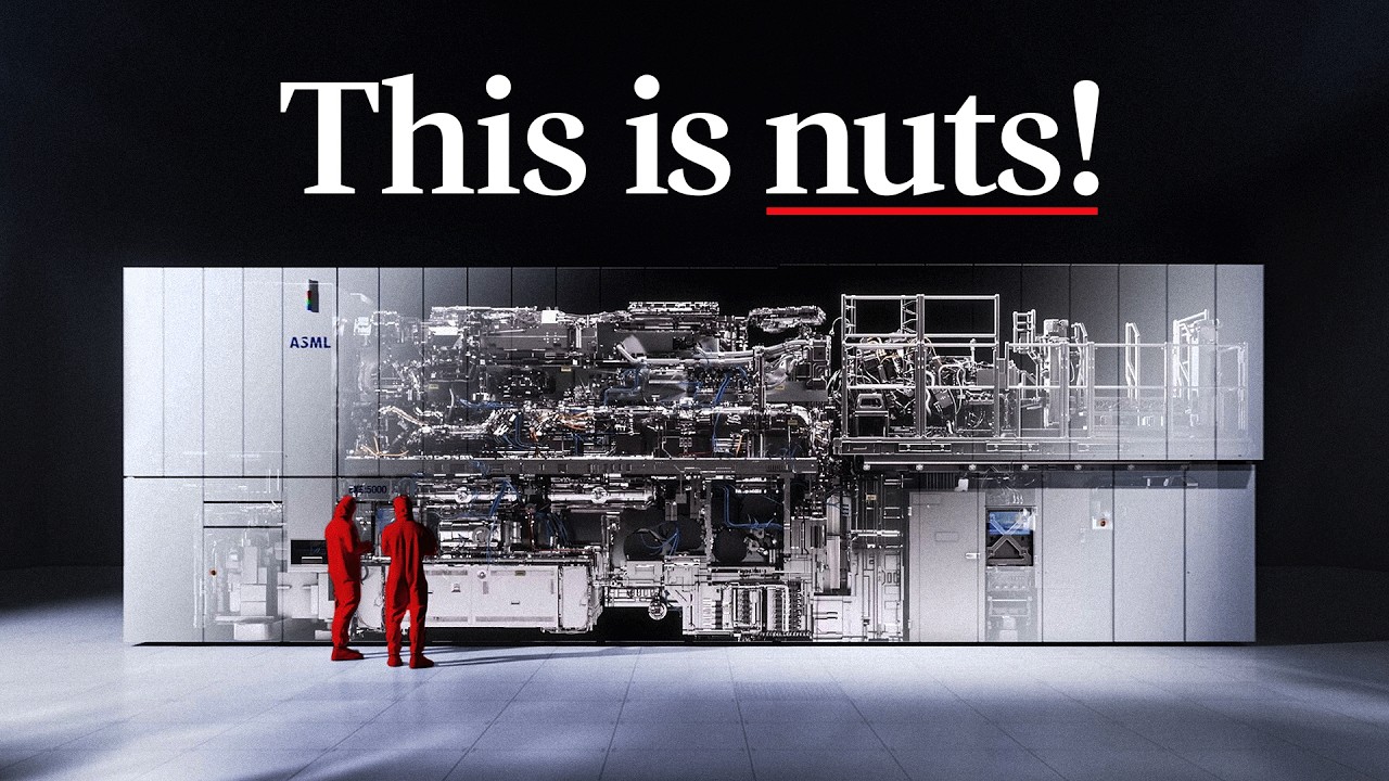
The Scale and Precision of ASML’s Machines
ASML’s EUV lithography machines are gargantuan and extraordinarily complex:
- They cost upwards of 350 million euros each.
- Constructed in ultra-clean rooms allowing only 10 particles per cubic meter (compared to 10,000 in hospital operating rooms).
- Contain thousands of parts sourced from over 5,000 suppliers.
- Utilize lasers amplified to 20,000 watts to vaporize tin droplets.
- Employ mirrors so smooth that if scaled to Earth size, their roughness would be thinner than a playing card.
- Achieve overlay precision of just one nanometer—the width of five silicon atoms—ensuring chip layers align perfectly despite the extreme accelerations (20 g’s) involved in reticle movement.
These machines are assembled, tested, disassembled, and shipped worldwide, involving 250 containers, 25 trucks, and seven Boeing 747 flights per high-NA machine.
Why ASML Is the Most Important Tech Company Today
Today, virtually all the world’s most advanced chips are manufactured using ASML’s EUV lithography machines. Their technology underpins the continued progress of Moore’s Law, enabling faster, more energy-efficient electronics that power smartphones, data centers, AI, and more.
Major semiconductor giants—Intel, Samsung, and TSMC—have invested billions into ASML’s development, recognizing that without EUV, the industry would stall.
Lessons from the Journey: Persistence, Innovation, and Unreasonable Determination
The three-decade journey to commercialize EUV lithography was fraught with skepticism, technical hurdles, and near-failures. Early pioneers like Kinoshita and Hawryluk were initially dismissed. Yet, their persistence, combined with breakthroughs in optics, plasma physics, and engineering, transformed an “impossible” idea into reality.
This story exemplifies how progress often depends on those who refuse to accept limits and adapt the world to their vision. It reminds us that breakthrough technologies are built on layers of knowledge, exploration, and relentless effort.
Learn More and Get Inspired
Understanding the science and engineering behind EUV lithography involves optics, materials science, plasma physics, and precision engineering. For those inspired to dive deeper into these fields or pursue their own big challenges, interactive learning platforms like Brilliant offer personalized courses in math, science, and computer science.
By learning how to break down complex problems and build skills, anyone can contribute to the next wave of technological breakthroughs.
In conclusion, ASML’s EUV lithography machines represent a pinnacle of human ingenuity, enabling the continuation of Moore’s Law and the rapid advancement of technology. This extraordinary machine is a testament to what can be achieved by combining visionary ideas, cutting-edge science, and unwavering determination.
If you’re fascinated by the intersection of science, technology, and innovation, the story of EUV lithography is one worth exploring—and a powerful reminder to stay curious and “unreasonable” in pursuit of progress.