YouTube Deep SummaryYouTube Deep Summary

Star Extract content that makes a tangible impact on your life

Video thumbnail

How are microchips made? - George Zaidan and Sajan Saini

TED-Ed • 2025-02-25 • 5:29 minutes • YouTube

🤖 AI-Generated Summary:

Inside the World of Computer Chip Manufacturing: A Marvel of Technology and Sustainability Challenges

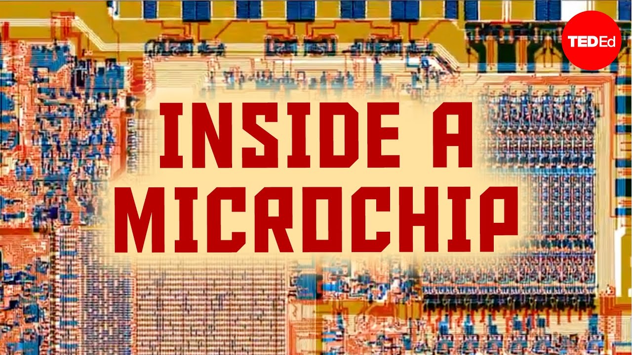
Have you ever wondered what goes into making the tiny computer chips that power our smartphones, laptops, and countless other devices? When magnified 500 times, a computer chip reveals a bustling “city” with distinct neighborhoods, interconnected by up to 100 kilometers of ultra-thin copper lines stacked across multiple layers. At the heart of this city are billions of transistors—tiny switches as small as 20 nanometers—that control the flow of electricity and enable complex digital functions.

The Scale of Chip Production

Globally, we produce more than a trillion computer chips every year. To put that into perspective, that’s about 20 trillion transistors built every single second, all manufactured in fewer than 500 fabrication plants known as fabs. But how are these incredibly tiny, intricately connected devices built so quickly and efficiently?

Photolithography: Building a City with Light

The answer lies in a fascinating technology called photolithography, which allows all the devices on a chip to be constructed simultaneously—imagine building an entire city’s buildings at once! This process uses light not just to illuminate but also to sculpt and measure at microscopic scales.

It all starts with a silicon wafer, which is carefully cleaned and oxidized to form a protective layer. A liquid called photoresist is then applied and baked to harden. Ultraviolet light shines through a specialized mask, selectively weakening the photoresist in certain areas. Chemicals wash away the weakened photoresist, leaving behind a precise pattern on the wafer. Then, reactive gases etch these patterns into the silicon surface, creating the intricate foundation of the chip’s circuitry.

Ions such as boron or phosphorus are implanted into these patterns to alter the silicon’s electrical properties, forming the essential transistor switches. However, the process leaves the surface uneven, requiring a high-precision polishing technique called Chemical Mechanical Polishing (CMP) to smooth the wafer before adding further layers.

The Complexity and Environmental Impact of Fabs

Fabrication plants operate around the clock, taking about three months to transform a pure silicon wafer into hundreds of finished chips. This continuous operation consumes enormous amounts of electricity, water, chemicals, acids, and precious metals. The wafers are processed in ultra-high purity environments maintained by constant vacuum pumps and filtered air systems to prevent contamination.

The cleaning and polishing processes generate significant liquid waste—nearly five gallons per wafer run from cleaning alone, plus five times more from slurry flushing during CMP. Additionally, fabs use vast quantities of nitrogen, helium, and other gases, some of which contribute to greenhouse emissions. To combat this, scrubber machines treat gaseous byproducts, but this treatment itself requires more water and energy.

Emerging Challenges and the Path Forward

As chips become more complex, they require more copper and precious metals for interconnections. Moreover, modern photoresists rely on PFAS chemicals, which are effective but pose environmental and health risks due to their persistence and accumulation in ecosystems and human bodies.

The demand for computer chips continues to rise, but fab operations are approaching sustainability limits. In some regions, water rationing prioritizes chip manufacturing over agriculture, highlighting the intense resource competition.

Towards Leaner, Cleaner, and Greener Chip Manufacturing

Computer chips are undoubtedly modern marvels that have transformed our world, and the fabs that build them are engineering wonders in their own right. However, the future of computing depends not only on advancing chip technology but also on innovating fab processes to be smarter, more efficient, and environmentally responsible.

Tomorrow’s fabs will need to minimize resource consumption, reduce waste and emissions, and embrace sustainable practices without compromising the precision and speed that define modern chip fabrication. Only by doing so can we ensure the continued growth of computing power while protecting our planet’s health.


In Conclusion

The intricate world of chip manufacturing reveals a delicate balance between technological advancement and environmental stewardship. Understanding the complexity behind every chip enhances our appreciation for the devices we use daily and underscores the importance of sustainable innovation in the semiconductor industry. As consumers and industry leaders alike, supporting and advocating for greener fabrication methods will help power a smarter, more sustainable future.

📝 Transcript (88 entries):

This is a computer chip, magnified 500 times. What you’re looking at is the top of a computing city, with distinct neighborhoods for different functions. They’re linked by up to 100 kilometers of ultra-thin copper lines, running across 10 or more stacked levels. At the very bottom, billions of electronic devices generate the digital traffic that pulses across the chip. The most common of these devices is called a transistor; it’s a switch that allows current to flow if it receives a voltage. Transistors can be as small as 20 nanometers, and more than 50 billion of them can fit on a single chip. Globally, we produce more than a trillion computer chips every year. That’s about 20 trillion transistors built every second, and it’s done in fewer than 500 fabrication plants, known as fabs. How do we build so many tiny, intricately-connected devices, so incredibly fast? The answer involves a technology called photolithography, which helps us build all the devices on a chip simultaneously. It’s like constructing all the buildings in a city at the same time. And with no tiny construction crews to help, we build using light as a measuring and sculpting tool. The process starts with a wafer of silicon, which is doused in solvents and acids to strip it clean before entering a furnace. Here, oxygen gas reacts with the wafer to form a layer of silicon dioxide. Then, a liquid called “photoresist” is spun on and baked to harden. Next, ultraviolet light selectively illuminates the wafer, by passing through or reflecting off a specialized mask. In the lit areas, a reaction weakens the photoresist’s chemical bonds. The wafer is doused in another chemical to wash away that weakened photoresist, leaving an image of the mask. And an etching machine’s reactive gases remove the exposed oxide, creating windows that drill the mask’s pattern down to the wafer surface. An implanter then accelerates boron or phosphorus ions and slams them into the patterned openings. These atoms form electropositive or electronegative regions that change silicon’s conductivity, creating the foundation of the transistor switch. The etched oxide windows, however, create hill-and-valley features. Before the next level of copper lines are added, this one’s uneven lines must be polished flat, to near-atomic precision, using a sophisticated grinding process called chemical mechanical polishing, or CMP. CMP uses a controlled slurry of sub-micron ceramic particles to gently scrape and flatten the bumpy features. These fab tools, and many others, are used hundreds of times on a wafer, to create and link transistors into computing logic gates, and to make connected neighborhoods for memory storage and computation. Fabs run around the clock, and it takes about three months to transform a single wafer from pure silicon into hundreds of chips. With this continuous operation, fabs consume huge amounts of electricity, water, solvents, acids, bases, process gases, and precious metals. Wafers are processed in ultra-high purity tool chambers, maintained by pumps running constantly, to sustain a vacuum that resembles deep space. High-temperature furnaces never turn off. Fab air handlers constantly expel filtered air to corral dust and tiny particles away from wafers. This takes a lot of electricity. The chemicals and purified water used in cleaning create nearly five gallons of waste per wafer run— which needs to be filtered and pH treated. Meanwhile, CMP slurries are continually flushed with water to keep their fine particles from forming chunks that would tear apart the fragile copper lines. This adds five times more liquid waste. Fabs plow through vast amounts of nitrogen and helium gas to run their tools. And other gases used and generated in these tools are greenhouse contributors. To minimize their emission, machines called scrubbers decompose and dissolve some gaseous byproducts into treatable wastewater. That uses more electricity, and more water. As computing complexity grows, more copper and precious metals are needed to link up chips. And new problems arise: today, PFAS-based photoresists are essential to make ever-smaller features. But PFAS waste in the environment is ending up in our bodies, and it may be harmful. Computer chips are modern marvels that have transformed our world— and the factories that build them are themselves engineering wonders. But as our demand for chips accelerates, their fabrication is hitting hard sustainability limits. Already, some places are beginning to ration water to farmers, in favor of running fabs. For the sake of the future of computing and our environment, tomorrow’s leaner, cleaner, and greener fabs will need to run even smarter than the very chips they build.